Loading...
News Article

Eta Research Develops Polished 100mm GaN Wafers

News

Chinese firm has grown MOCVD GaN epi-layers and device structures on the wafers

Eta Research, a Chinese semiconductor company with headquarters in the new Lingang Free Trade Zone of Shanghai, is now selling n-type 100 mm GaN wafers with an epitaxial ready polish.

Eta Research uses the HVPE method to produce GaN wafers. The company says it has completed the R&D necessary for commercialisation of GaN wafers resulting in its HVPE equipment, wafer separation process, and polishing process. In 2018, the company demonstrated as-grown GaN wafers of 100 mm diameter which can be cut to 2 inch and 3 inch wafers as the finished size. In 2019, the company has developed nearly 5inch as-grown GaN wafers which can be cut and processed into 100 mm wafers.

The company says it puts a strong emphasis on the importance of the crystal quality and lattice curvature. The typical rocking curve FWHMs of the as-grown wafers are 50 to 60 arcsec for both the (002) and (102) reflections. The threading dislocation density has been measured as 1E6 /cm2 based on CL of polished wafers. The lattice curvature is important as a measure of the offcut variation across the wafer. The center point offcut is specified at 0.35° toward the GaN m-direction and that can be modified according to the customer’s requirement. The lattice curvature radius is greater than 10 m, with the target around 30 m or larger.

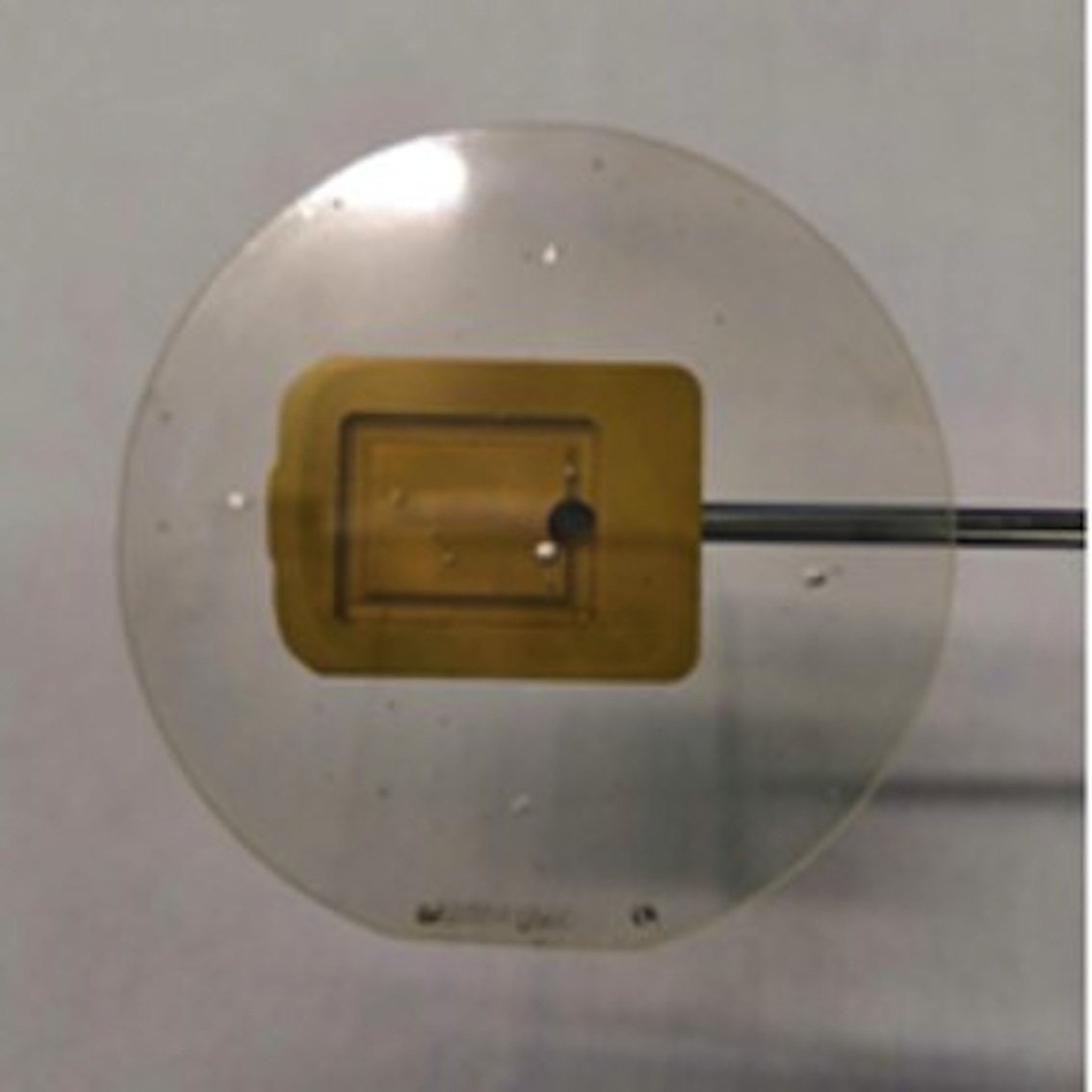
The company has developed their own polishing process for GaN, resulting in AFM average roughness over 10µm images of < 0.3 nm. It has grown MOCVD GaN epi-layers and device structures on the GaN wafers (pictured above is an LED epi wafer). Eta Research says that the MOCVD-grown layers show good surface morphology and have XRD rocking curve FWHMs similar to that of the substrate.

Currently, small quantities of 100 mm GaN wafers are for sale, as well as 2 inch and 3 inch wafers. At the end of 2019, more HVPE capacity will be brought online in the new production factory located in Tongling, Anhui Province, China. ET Research anticipates the ability to supply high volume customers in the near future. Furthermore, working with their epitaxial growth partners, Eta Research can offer GaN wafers with MOCVD epitaxial layers for interested customers.

SPONSOR MESSAGE

Secure Your Hydrogen Supply

A study supply of high-purity hydrogen is critical to semiconductor fabrication. Supply chain interruptions are challenging manufacturers, leading to production slowdowns and stoppages. On-site hydrogen generation offers a scalable alternative for new and existing fabs, freeing the operator from dependence on delivered gas.

Plant managers understand the critical role that hydrogen plays in semiconductor fabrication. That important job includes crystal growth, carrier gas, wafer annealing, and in the emerging Extreme UV Lithography (EUV) that will enable new generations of devices. As the vast need for semiconductors grows across all sectors of world economies, so does the need for high-purity hydrogen.

Take control with Nel on-site hydrogen generation.

Read more
SiC MOSFETs: Understanding the benefits of plasma nitridation
Wolfspeed reports Q2 results
VueReal secures $40.5m to scale MicroSolid printing
Mitsubishi joins Horizon Europe's FLAGCHIP project
Vishay launches new high voltage SiC diodes
UK team leads diamond-FET breakthrough
GaN adoption at tipping point, says Infineon
BluGlass files tuneable GaN laser patents
QD company Quantum Science expands into new facility
Innoscience files lawsuit against Infineon
Riber revenues up 5% to €41.2m
Forvia Hella to use CoolSiC for next generation charging
Photon Design to exhibit QD simulation tool
Ortel transfers CW laser fabrication to Canada
Luminus adds red and blue multi-mode Lasers
PseudolithIC raises $6M for heterogeneous chiplet tech
Mesa sidewall design improves HV DUV LEDs
IQE revenue to exceed expectations
'Game-changing' VCSEL system targets clinical imaging
German start-up secures finance for SiC processing tech
Macom signs preliminaries for CHIPS Act funding
IQE and Quintessent partner on QD lasers for AI
EU funds perovskite tandems for fuel-free space propulsion
EU to invest €3m in GeSi quantum project
Transforming the current density of AlN Schottky barrier diodes
Turbocharging the GaN MOSFET with a HfO₂ gate
Wolfspeed launches Gen 4 SiC MOSFET technology
Report predicts high growth for UK's North East
Element Six unveils Cu-diamond composite
SemiQ launches hi-rel 1700V SiC MOSFETs
Lynred to exhibit Eyesential SWIR sensor for machine vision
Thorlabs buys VCSEL firm Praevium Research
×
Search the news archive

To close this popup you can press escape or click the close icon.
Logo
x
Logo
×
Register - Step 1

You may choose to subscribe to the Compound Semiconductor Magazine, the Compound Semiconductor Newsletter, or both. You may also request additional information if required, before submitting your application.


Please subscribe me to:


You chose the industry type of "Other"

Please enter the industry that you work in:
 
x
Adblocker Detected
Please consider unblocking adverts on this website